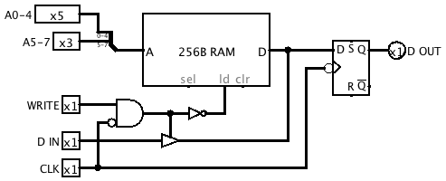
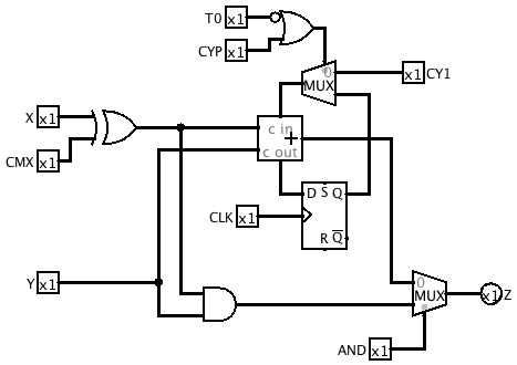
| CYP |
CY1 |
CMX |
AND |
Result |
| 0 |
0 |
0 |
0 |
Y + X |
| 0 |
1 |
0 |
0 |
Y + X + 1 |
| 1 |
x |
0 |
0 |
Y + X with carry in |
| 0 |
1 |
1 |
0 |
Y - X |
| 0 |
0 |
1 |
0 |
Y - X - 1 |
| 1 |
x |
1 |
0 |
Y - X with carry in |
| x |
x |
x |
1 |
Y AND X |
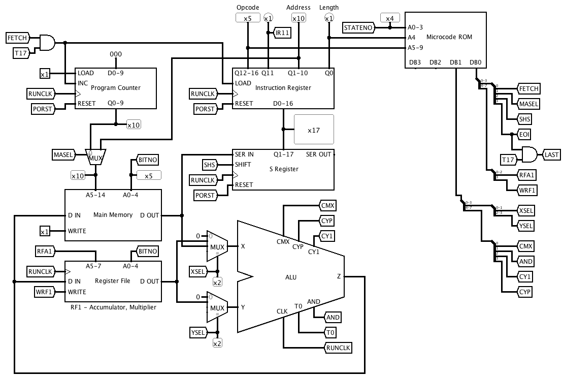
| EOI | End of Instruction |
Indicates the last short word cycle of an instruction. Causes LAST to be activated during T17. |
| RFA1 |
Register File 1 Address |
Selects one of 8 short words in Register File 1. |
| WRF1 |
Write Register File 1 |
Causes the output of the ALU to be written into Register File 1. |
| XSEL |
X Select |
Selects the source for ALU input X. |
| YSEL |
Y Select |
Selects the source for ALU input Y. |
| CMX |
Complement X |
ALU control inputs |
| AND |
Logical AND |
|
| CY1 |
Carry in value |
|
| CYP |
Use previous carry |
| 00 |
Constant 0 |
| 01 |
Register File 1 |
| 10 |
Main Memory |
| 11 |
Currently unused |
| 00 |
Constant 0 |
| 01 |
Register File 1 |
| 10 |
Currently unused |
| 11 |