Right Shift Instruction
I spent quite a long time thinking about how to implement this
instruction. The strategy I eventually came up with is to add 1 to the
register file address during the read phase of each bit time. So it
reads bit 1 and writes it to bit 0, reads bit 2 and writes it to bit 1,
etc. A fair bit of extra circuitry will be required to achieve this,
and I don't really like the idea of adding that much complexity just to
support one operation, but I haven't been able to think of a simpler
way without radically changing the whole design.
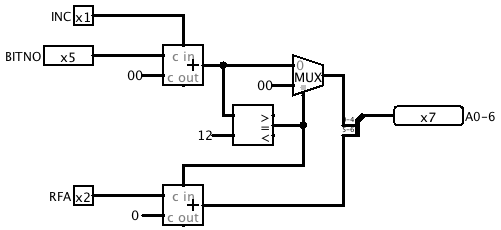
This is the subcircuit I designed to carry out the address
incrementing. When the INC input is activated, a 5-bit adder adds 1 to
BITNO. If the result is 18 (0x12) the result is forced to zero and a
carry is added to RFA.
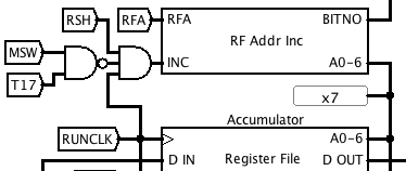
Here's where it fits into the main circuit. A new control signal RSH
enables right-shifting behaviour. It is gated with RUNCLK so that the
register file address is incremented during the read phase of each bit
time. Incrementing is disabled during T17 of the most significant word,
so that the most significant bit is unaltered. This makes the operation
an arithmetic shift (i.e. with sign extension).
Microcode
This is the microcode for the right shift instruction. It uses the same
technique as the left shift for keeping track of the number of places
to shift.
# OPCODE L STAT : FETCH MASEL SHS EOI RFA WRF XSEL YSEL  CMX SS1 CY1 CYP ODD MSW LSW HALT WMEM UBCOND UBADDR RSH

# R - Right shift
   00100 x 0001 :   0     0    0   0   00  10   10   00   0   0   0   0   0   0   1   0    0    000    0000   1
   00100 x 0010 :   0     0    0   0   10  10   10   00   0   0   0   0   0   0   0   0    0    000    0000   1
   00100 x 0011 :   0     0    0   0   01  10   10   00   0   0   0   0   0   0   0   0    0    000    0000   1
   00100 x 0100 :   0     0    0   1   11  10   10   00   0   1   0   0   0   1   0   0    0    100    1000   1
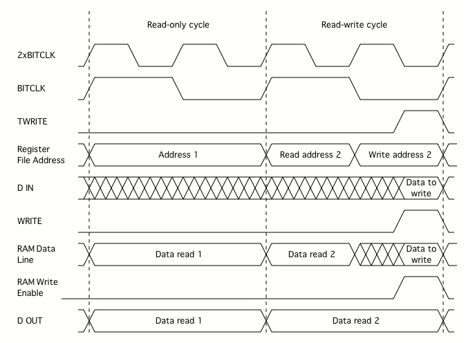
Glitches, Will Robinson!
Testing in Logisim revealed a problem with this arrangement.
Previously, the register address only changed on the rising edge of
BITCLK, and was stable at the leading edge of the WRITE signal to the
register file, but now the register address can also change on the
falling edge of BITCLK. This was causing spurious bits in the
accumulator to change.
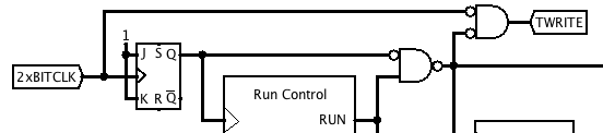
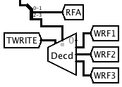
To fix this, I changed the clocking arrangement. The simulation is now
clocked at twice the BITCLK rate, and a timing signal TWRITE is derived
that is active during the last quarter of each bit period. This is used
to gate the WRF1-WRF3 signals, which delays writing to the register
file until a quarter of a bit period after any potential address change.
Revised register file timing: